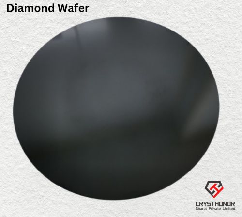
Diamond Wafer
Used as a heat spreader or substrate for high-power electronic devices.
Avilable sizes- 1”- 6”
Applications of Diamond Wafers:
- Semiconductors & Electronics – Used as a heat spreader or substrate for high-power electronic devices.
- Optics & Lasers – Utilized in infrared and high-power laser windows.
- Cutting & Grinding Tools – Employed in precision machining for its extreme hardness.
- Quantum Computing – Used in diamond-based quantum sensors and computing.
1. Monocrystalline Diamond Wafer
- Made from a single continuous crystal of diamond.
- Has a uniform structure with no grain boundaries.
- Offers higher purity, thermal conductivity, and mechanical strength than polycrystalline wafers.
- Used in semiconductors, optics, and quantum computing.
- More expensive due to the complex growth process, typically done using chemical vapor deposition (CVD) or high-pressure high-temperature (HPHT) methods.
2. Polycrystalline Diamond Wafer
- Made up of multiple diamond grains fused together.
- Contains grain boundaries, which may slightly reduce thermal conductivity and strength compared to monocrystalline.
- More cost-effective and easier to manufacture in larger sizes.
- Commonly used in cutting tools, heat spreaders, and industrial coatings.
- Typically produced using chemical vapor deposition (CVD).
|
Feature |
Monocrystalline Diamond |
Polycrystalline Diamond |
|---|---|---|
|
Crystal Structure |
Single crystal |
Multiple grains |
|
Purity & Strength |
Higher |
Slightly lower |
|
Thermal Conductivity |
Higher |
Slightly lower |
|
Manufacturing Cost |
More expensive |
More affordable |
|
Applications |
High-end electronics, quantum tech, optics |
Cutting tools, heat spreaders, industrial use |


